Мощное охлаждение для оптимизации производительности схемы и затрат
Thermal simulation is an important part of developing power products and providing product material guidelines. Optimizing the size of the module is the development trend of terminal equipment design, which brings about the conversion of heat dissipation management from the metal heat sink to the PCB copper layer. Some modules today use lower switching frequencies for switch-mode power supplies and large passive components. For the voltage conversion and quiescent current driving the internal circuit, the efficiency of the linear regulator is relatively low.
As the functions become more abundant, the performance becomes higher and higher, and the device design becomes increasingly compact. At this time, IC-level and system-level heat dissipation simulation becomes very important.
The working environment temperature of some applications is 70 to 125 degree , and the temperature of some die-size automotive applications is even as high as 140 degree . For these applications, the uninterrupted operation of the system is very important. When optimizing electronic designs, accurate thermal analysis under transient and static worst-case scenarios for the above two types of applications is becoming increasingly important.
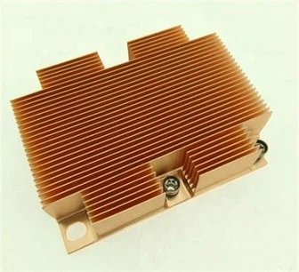
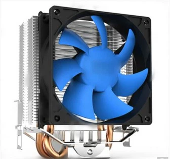
The heat dissipation and thermal resistance paths are different according to different implementation methods: The heat dissipation pads connected to the internal heat sink panel or the heat dissipation holes at the junction of the protrusions. Use solder to connect the exposed thermal pad or bump connection to the top layer of the PCB. An opening on the PCB below the exposed thermal pad or bump connection, which can be connected to the extended heat sink base connected to the module's metal casing. Use metal screws to connect the heat sink to the heat sink on the top or bottom copper layer of the PCB of the metal shell. Use solder to connect the exposed thermal pad or bump connection to the top layer of the PCB. In addition, the weight or thickness of the copper plating used on each layer of the PCB is very critical. In terms of thermal resistance analysis, the layers connected to the exposed pads or bumps are directly affected by this parameter. Generally speaking, these are the top, heat sink, and bottom layers in a multilayer printed circuit board. In most applications, it can be a two{{0}}ounce copper (2 ounce copper = 2.8 mils or 71 µm) outer layer, and a 1-ounce copper (1 ounce copper = 1.4 mils or 35 µm) inner layer, or all All are 1 ounce heavy copper clad layer. In consumer electronics applications, some applications even use 0.5 ounces of copper (0.5 ounces of copper = 0.7 mils or 18 µm) layer.
")
Model data
Simulating the die temperature requires an IC layout diagram, which includes all the power FETs on the die and the actual positions that comply with the packaging and soldering principles.
The size and aspect ratio of each FET are very important for heat distribution. Another important factor to consider is whether the FETs are powered up simultaneously or sequentially. The accuracy of the model depends on the physical data and material properties used. The static or average power analysis of the model requires only a short calculation time, and convergence occurs once the maximum temperature is recorded.
Transient analysis requires power-time comparison data. We used a better analytical procedure than the switching power supply case to record the data to accurately capture the peak temperature rise during fast power pulses. This type of analysis is generally time-consuming and requires more data input than static power simulation.
This model can simulate the epoxy pores in the die connection area, or the plating pores of the PCB heat sink. In both cases, epoxy/plating pores will affect the thermal resistance of the package.
Thermal simulation is an important part of the development of power products. In addition, it can also guide you to set the thermal resistance parameters, covering the entire range from the silicon chip FET junction to the implementation of various materials in the product. Once we understand the different thermal resistance paths, we can optimize many systems for all applications.
This data can also be used to determine the correlation between the derating factor and the increase in ambient operating temperature. These results can be used to help product development teams develop their designs.
")